 | –≠–ª–µ–∫—Ç—Ä–æ–Ω–Ω—ã–π –∫–æ–º–ø–æ–Ω–µ–Ω—Ç: OPA2336PA | –°–∫–∞—á–∞—Ç—å:  PDF PDF  ZIP ZIP |
FEATURES
q
SINGLE-SUPPLY OPERATION
q
RAIL-TO-RAIL OUTPUT (within 3mV)
q
micro
POWER: I
Q
= 20
µ
A/Amplifier
q
micro
SIZE PACKAGES
q
LOW OFFSET VOLTAGE: 125
µ
V max
q
SPECIFIED FROM V
S
= 2.3V to 5.5V
q
SINGLE, DUAL, AND QUAD VERSIONS
OPA336
OPA2336
OPA4336
SINGLE-SUPPLY,
micro
Power
CMOS OPERATIONAL AMPLIFIERS
micro
Amplifier
TM
Series
APPLICATIONS
q
BATTERY-POWERED INSTRUMENTS
q
PORTABLE DEVICES
q
HIGH-IMPEDANCE APPLICATIONS
q
PHOTODIODE PRE-AMPS
q
PRECISION INTEGRATORS
q
MEDICAL INSTRUMENTS
q
TEST EQUIPMENT
DESCRIPTION
OPA336 series
microPower CMOS operational amplifiers
are designed for battery-powered applications. They
operate on a single supply with operation as low as 2.1V.
The output is rail-to-rail and swings to within 3mV of the
supplies with a 100k
load. The common-mode range
extends to the negative supply--ideal for single-supply
applications. Single, dual, and quad versions have identical
specifications for maximum design flexibility.
In addition to small size and low quiescent current
(20
µ
A/amplifier), they feature low offset voltage
(125
µ
V max), low input bias current (1pA), and high open-
loop gain (115dB). Dual and quad designs feature
completely independent circuitry for lowest crosstalk and
freedom from interaction.
OPA336 packages are the tiny SOT23-5 surface mount
and SO-8 surface-mount. OPA2336 come in the miniature
MSOP-8 surface-mount, SO-8 surface-mount, and DIP-8
packages. The OPA4336 package is the space-saving
SSOP-16 surface-mount. All are specified from
≠40
∞
C to +85
∞
C and operate from ≠55
∞
C to +125
∞
C.
A macromodel is available for download (at www.ti.com)
for design analysis.
OPA4
336
OPA3
36
OPA2
336
SBOS068B ≠ JANUARY 1997 ≠ REVISED APRIL 2004
www.ti.com
PRODUCTION DATA information is current as of publication date.
Products conform to specifications per the terms of Texas Instruments
standard warranty. Production processing does not necessarily include
testing of all parameters.
Copyright © 1997-2004, Texas Instruments Incorporated
Please be aware that an important notice concerning availability, standard warranty, and use in critical applications of
Texas Instruments semiconductor products and disclaimers thereto appears at the end of this data sheet.
All trademarks are the property of their respective owners.
1
2
3
5
4
V+
≠In
Out
V≠
+In
OPA336
SOT23-5
1
2
3
4
8
7
6
5
NC
V+
Output
NC
NC
≠In
+In
V≠
OPA336
SO-8
NC = No Connection
1
2
3
4
8
7
6
5
V+
Out B
≠In B
+In B
Out A
≠In A
+In A
V≠
OPA2336
DIP-8, SO-8, MSOP-8
A
B
1
2
3
4
5
6
7
8
16
15
14
13
12
11
10
9
Out D
≠In D
+In D
V≠
+In C
≠In C
Out C
NC
Out A
≠In A
+In A
V+
+In B
≠In B
Out B
NC
OPA4336
A
D
B
C
SSOP-16
NC = No Connection
OPA336, 2336, 4336
2
SBOS068B
www.ti.com
PACKAGE
SPECIFIED
DRAWING
TEMPERATURE
PACKAGE
ORDERING
TRANSPORT
PRODUCT
PACKAGE-LEAD
DESIGNATOR
RANGE
MARKING
NUMBER
(1)
MEDIA, QUANTITY
Single
OPA336N
SOT23-5
DBV
≠40
∞
C to +85
∞
C
A36
(2)
OPA336N/250
Tape and Reel, 250
"
"
"
"
"
OPA336N/3K
Tape and Reel, 3000
OPA336NA
SOT23-5
DBV
≠40
∞
C to +85
∞
C
A36
(2)
OPA336NA/250
Tape and Reel, 250
"
"
"
"
"
OPA336NA/3K
Tape and Reel, 3000
OPA336NJ
SOT23-5
DBV
≠40
∞
C to +85
∞
C
J36
OPA336NJ/250
Tape and Reel, 250
"
"
"
"
"
OPA336NJ/3K
Tape and Reel, 3000
OPA336U
SO-8 Surface-Mount
D
≠40
∞
C to +85
∞
C
OPA336U
OPA336U
Rails
(3)
, 100
"
"
"
"
"
OPA336U/2K5
Tape and Reel, 2500
OPA336UA
SO-8 Surface-Mount
D
≠40
∞
C to +85
∞
C
OPA336UA
OPA336UA
Rails
(3)
, 100
"
"
"
"
"
OPA336UA/2K5
Tape and Reel, 2500
OPA336UJ
(4)
SO-8 Surface-Mount
D
≠40
∞
C to +85
∞
C
OPA336UJ
OPA336UJ
Rails
(3)
, 100
"
"
"
"
"
OPA336UJ/2K5
Tape and Reel, 2500
Dual
OPA2336E
MSOP-8 Surface-Mount
DGK
≠40
∞
C to +85
∞
C
B36
(2)
OPA2336E/250
Tape and Reel, 250
"
"
"
"
"
OPA2336E/2K5
Tape and Reel, 2500
OPA2336EA
MSOP-8 Surface-Mount
DGK
≠40
∞
C to +85
∞
C
B36
(2)
OPA2336EA/250
Tape and Reel, 250
"
"
"
"
"
OPA2336EA/2K5
Tape and Reel, 2500
OPA2336P
DIP-8
P
≠40
∞
C to +85
∞
C
OPA2336P
OPA2336P
Rails, 50
OPA2336PA
DIP-8
P
≠40
∞
C to +85
∞
C
OPA2336PA
OPA2336PA
Rails, 50
OPA2336U
SO-8 Surface-Mount
D
"
OPA2336U
OPA2336U
Rails
(3)
, 100
"
"
"
"
"
OPA2336U/2K5
Tape and Reel, 2500
OPA2336UA
SO-8 Surface-Mount
D
≠40
∞
C to +85
∞
C
OPA2336UA
OPA2336UA
Rails
(3)
, 100
"
"
"
"
"
OPA2336UA/2K5
Tape and Reel, 2500
Quad
OPA4336EA
SSOP-16 Surface-Mount
DBQ
≠40
∞
C to +85
∞
C
OPA4336EA
OPA4336EA/250
Tape and Reel, 250
"
"
"
"
"
OPA4336EA/2K5
Tape and Reel, 2500
NOTES: (1) For the most current package and ordering information, see the package option addendum at the end of this data sheet. (2) Grade will be marked on
the Reel. (3) SO-8 models also available in Tape and Reel. (4) Available Q2, 2004.
PACKAGE/ORDERING INFORMATION
(1)
ELECTROSTATIC
DISCHARGE SENSITIVITY
This integrated circuit can be damaged by ESD. Texas
Instruments recommends that all integrated circuits be handled
with appropriate precautions. Failure to observe proper han-
dling and installation procedures can cause damage.
ESD damage can range from subtle performance degrada-
tion to complete device failure. Precision integrated circuits
may be more susceptible to damage because very small
parametric changes could cause the device not to meet its
published specifications.
Supply Voltage ................................................................................... 7.5V
Signal Input Terminals, Voltage
(2)
..................... (V≠) ≠0.3V to (V+) +0.3V
Current
(2)
.................................................... 10mA
Output Short-Circuit
(3)
.............................................................. Continuous
Operating Temperature .................................................. ≠55
∞
C to +125
∞
C
Storage Temperature ..................................................... ≠55
∞
C to +125
∞
C
Junction Temperature ...................................................................... 150
∞
C
Lead Temperature (soldering, 10s) ................................................. 300
∞
C
NOTES: (1) Stresses above these ratings may cause permanent damage.
Exposure to absolute maximum conditions for extended periods may
degrade device reliability. These are stress ratings only. Functional opera-
tion of the device at these conditions, or beyond the specified operating
conditions, is not implied. (2) Input terminals are diode-clamped to the power
supply rails. Input signals that can swing more than 0.3V beyond the supply
rails should be current-limited to 10mA or less. (3) Short-circuit to ground,
one amplifier per package.
ABSOLUTE MAXIMUM RATINGS
(1)

OPA336, 2336, 4336
3
SBOS068B
www.ti.com
ELECTRICAL CHARACTERISTICS: V
S
= 2.3V to 5.5V
Boldface
limits apply over the specified temperature range,
T
A
= ≠40
∞
C to +85
∞
C
.
At T
A
= +25
∞
C, V
S
= +5V, and R
L
= 25k
connected to V
S
/2, unless otherwise noted.
OPA336NA, UA
OPA336N, U
OPA2336EA, PA, UA
OPA2336E, P, U
OPA4336EA
OPA336NJ, UJ
PARAMETER
CONDITION
MIN
TYP
(1)
MAX
MIN
TYP
MAX
MIN
TYP MAX
UNITS
OFFSET VOLTAGE
Input Offset Voltage
V
OS
±
60
±
125
±
500
±
500
±
2500
µ
V
vs Temperature
dV
OS
/dT
±
1.5
µ
V/
∞
C
vs Power Supply
PSRR
V
S
= 2.3V to 5.5V
25
100
µ
V/V
Over Temperature
V
S
= 2.3V to 5.5V
130
µ
V/V
Channel Separation, dc
0.1
µ
V/V
INPUT BIAS CURRENT
Input Bias Current
I
B
±
1
±
10
pA
Over Temperature
±
60
pA
Input Offset Current
I
OS
±
1
±
10
pA
NOISE
Input Voltage Noise, f = 0.1 to 10Hz
3
µ
Vp-p
Input Voltage Noise Density, f = 1kHz e
n
40
nV/
Hz
Current Noise Density, f = 1kHz
i
n
30
fA/
Hz
INPUT VOLTAGE RANGE
Common-Mode Voltage Range
V
CM
≠0.2
(V+) ≠1
V
Common-Mode Rejection Ratio
CMRR
≠0.2V < V
CM
< (V+) ≠1V
80
90
76
86
76
86
dB
Over Temperature
≠0.2V < V
CM
< (V+) ≠1V
76
74
74
dB
INPUT IMPEDANCE
Differential
10
13
|| 2
|| pF
Common-Mode
10
13
|| 4
|| pF
OPEN-LOOP GAIN
Open-Loop Voltage Gain
A
OL
R
L
= 25k
, 100mV < V
O
< (V+) ≠ 100mV
100
115
90
90
dB
Over Temperature
R
L
= 25k
, 100mV < V
O
< (V+) ≠ 100mV
100
90
90
dB
R
L
= 5k
, 500mV < V
O
< (V+) ≠ 500mV
90
106
dB
Over Temperature
R
L
= 5k
, 500mV < V
O
< (V+) ≠ 500mV
90
dB
FREQUENCY RESPONSE
Gain-Bandwidth Product
GBW
V
S
= 5V, G = 1
100
kHz
Slew Rate
SR
V
S
= 5V, G = 1
0.03
V/
µ
s
Overload Recovery Time
V
IN
∑ G = V
S
100
µ
s
OUTPUT
Voltage Output Swing from Rail
(2)
R
L
= 100k
, A
OL
70dB
3
mV
R
L
= 25k
,
A
OL
90dB
20
100
mV
Over Temperature
R
L
= 25k
,
A
OL
90dB
100
mV
R
L
= 5k
, A
OL
90dB
70
500
mV
Over Temperature
R
L
= 5k
, A
OL
90dB
500
mV
Short-Circuit Current
I
SC
±
5
mA
Capacitive Load Drive
C
LOAD
See Text
pF
POWER SUPPLY
Specified Voltage Range
V
S
2.3
5.5
V
Minimum Operating Voltage
2.1
V
Quiescent Current (per amplifier)
I
Q
I
O
= 0
20
32
23
38
µ
A
Over Temperature
I
O
= 0
36
42
µ
A
TEMPERATURE RANGE
Specified Range
≠40
+85
∞
C
Operating Range
≠55
+125
∞
C
Storage Range
≠55
+125
∞
C
Thermal Resistance
JA
SOT-23-5 Surface-Mount
200
∞
C/W
MSOP-8 Surface-Mount
150
∞
C/W
SO-8 Surface-Mount
150
∞
C/W
DIP-8
100
∞
C/W
SSOP-16 Surface-Mount
100
∞
C/W
DIP-14
80
∞
C/W
Specifications same as OPA2336E, P, U.
NOTES: (1) V
S
= +5V. (2) Output voltage swings are measured between the output and positive and negative power-supply rails.
OPA336, 2336, 4336
4
SBOS068B
www.ti.com
TYPICAL CHARACTERISTICS
At T
A
= +25
∞
C, V
S
= +5V, and R
L
= 25k
connected to V
S
/2, unless otherwise noted.
OPEN-LOOP GAIN/PHASE vs FREQUENCY
1
100
80
60
40
20
0
≠20
Voltage Gain (dB)
0
≠45
≠90
≠135
≠180
Phase (
∞
)
Frequency (Hz)
10
100
1k
10k
100k
1M
G
SHORT-CIRCUIT CURRENT vs SUPPLY VOLTAGE
Supply Voltage (V)
Short-Circuit Current (mA)
±6
±5
±4
±3
±2
±1
0
2.0
2.5
3.0
3.5
4.0
4.5
5.0
5.5
6.0
+I
SC
≠I
SC
POWER-SUPPLY and COMMON-MODE
REJECTION RATIO vs FREQUENCY
100
80
60
40
20
0
PSRR, CMRR (dB)
Frequency (Hz)
1
10
100
1k
10k
100k
CMRR
PSRR
SHORT-CIRCUIT CURRENT vs TEMPERATURE
Temperature (
∞
C)
Short-Circuit Current (mA)
8
7
6
5
4
3
2
1
0
≠75
≠50
≠25
0
25
50
75
100
125
V
S
= +2.3V
V
S
= +5V
≠I
SC
+I
SC
+I
SC
≠I
SC
QUIESCENT CURRENT vs SUPPLY VOLTAGE
Supply Voltage (V)
Quiescent Current (
µ
A)
30
25
20
15
10
2.0
2.5
3.0
3.5
4.0
4.5
5.0
5.5
6.0
Per Amplifier
QUIESCENT CURRENT vs TEMPERATURE
Temperature (
∞
C)
Quiescent Current (
µ
A)
30
25
20
15
10
5
0
≠75
≠50
≠25
0
25
50
75
100
125
V
S
= +2.3V
V
S
= +5V
Per Amplifier
OPA336, 2336, 4336
5
SBOS068B
www.ti.com
TYPICAL CHARACTERISTICS
(Cont.)
At T
A
= +25
∞
C, V
S
= +5V, and R
L
= 25k
connected to V
S
/2, unless otherwise noted.
MAXIMUM OUTPUT VOLTAGE vs FREQUENCY
100k
10k
Frequency (Hz)
100
1k
6
5
4
3
2
1
0
Output Voltage (Vp-p)
V
S
= +5.5V
V
S
= +2.3V
OFFSET VOLTAGE
PRODUCTION DISTRIBUTION
Percent of Amplifiers (%)
Offset Voltage (
µ
V)
≠
500
≠
400
≠
300
≠
200
≠
100
0
100
200
300
400
500
25
20
15
10
5
0
0.1%
0.2%
0.3%
0.1%
Typical production
distribution of
packaged units.
A
OL
, CMRR, PSRR vs TEMPERATURE
Temperature (∞C)
A
OL
, CMRR, PSRR (dB)
120
110
100
90
80
70
≠75
≠50
≠25
0
25
50
75
100
125
A
OL
PSRR
CMRR
OFFSET VOLTAGE DRIFT MAGNITUDE
PRODUCTION DISTRIBUTION
Percent of Amplifiers (%)
Offset Voltage Drift (
µ
V/
∞
C)
0.25
0.5
0.75
1
1.25
1.5
1.75
2
2.25
2.5
2.75
3
3.25
3.5
3.75
4
25
20
15
10
5
0
Typical production
distribution of
packaged units.
INPUT VOLTAGE AND CURRENT NOISE
SPECTRAL DENSITY vs FREQUENCY
Frequency (Hz)
1k
100
10
1
1k
100
10
1
10
100
1k
10k
100k
Voltage Noise (nV/
Hz)
Current Noise (fA/
Hz)
Voltage Noise
Current Noise
CHANNEL SEPARATION vs FREQUENCY
Frequency (Hz)
Channel Separation (dB)
150
140
130
120
110
100
1k
10k
100k
Dual and Quad devices, G = 1, all
channels. Quad measured channel A
to D or B to C--other combinations
yield improved rejection.

OPA336, 2336, 4336
6
SBOS068B
www.ti.com
LARGE-SIGNAL STEP RESPONSE
G = 1, C
L
= 620pF, V
S
= +5V
200
µ
s/div
500mV/div
SMALL-SIGNAL STEP RESPONSE
G = 1, C
L
= 200pF, V
S
= +5V
50
µ
s/div
20mV/div
OUTPUT VOLTAGE SWING vs OUTPUT CURRENT
Output Voltage (V)
Output Current (mA)
≠0
≠1
≠2
≠3
≠4
≠5
≠6
≠7
≠8
≠2.5
≠2.0
≠1.5
≠1.0
≠0.5
0
Sinking
Current
+25
∞
C
≠55
∞
C
+125
∞
C
V
S
=
±
2.5V
OUTPUT VOLTAGE SWING vs OUTPUT CURRENT
Output Voltage (V)
Output Current (mA)
0
1
2
3
4
5
6
7
8
5
4
3
2
1
0
Sourcing
Current
≠55
∞
C
+25
∞
C
+125
∞
C
+125
∞
C
+25
∞
C
≠55
∞
C
V
S
= +2.3V
V
S
= +5V
INPUT BIAS CURRENT
vs INPUT COMMON-MODE VOLTAGE
Input Bias Current (pA)
Common-Mode Voltage (V)
0
1
2
3
4
5
4
3
2
1
0
V
S
= +5V
INPUT BIAS CURRENT vs TEMPERATURE
Input Bias Current (pA)
Temperature (∞C)
≠75
≠50
≠25
0
25
50
75
100
125
1k
100
10
1
0.1
TYPICAL CHARACTERISTICS
(Cont.)
At T
A
= +25
∞
C, V
S
= +5V, and R
L
= 25k
connected to V
S
/2, unless otherwise noted.
OPA336, 2336, 4336
7
SBOS068B
www.ti.com
CAPACITIVE LOAD AND STABILITY
OPA336 series op amps can drive a wide range of capaci-
tive loads. However, all op amps under certain conditions
may become unstable. Op-amp configuration, gain, and
load value are just a few of the factors to consider when
determining stability.
When properly configured, OPA336 series op amps can
drive approximately 10,000pF. An op amp in unity-gain
configuration is the most vulnerable to capacitive load. The
capacitive load reacts with the op amp's output resistance,
along with any additional load resistance, to create a pole in
the response which degrades the phase margin. In unity gain,
OPA336 series op amps perform well with a pure capacitive
load up to about 300pF. Increasing gain enhances the
amplifier's ability to drive loads beyond this level.
One method of improving capacitive load drive in the
unity-gain configuration is to insert a 50
to 100
resistor
inside the feedback loop, as shown in Figure 3. This reduces
ringing with large capacitive loads while maintaining DC
R
S
100
OPAx336
C
L
R
L
V
IN
V
OUT
APPLICATIONS INFORMATION
OPA336 series op amps are fabricated on a state-of-the-art
0.6 micron CMOS process. They are unity-gain stable and
suitable for a wide range of general-purpose applications.
Power-supply pins should be bypassed with 0.01
µ
F ceramic
capacitors. OPA336 series op amps are protected against
reverse battery voltages.
OPERATING VOLTAGE
OPA336 series op amps can operate from a +2.1V to +5.5V
single supply with excellent performance. Most behavior
remains unchanged throughout the full operating voltage
range. Parameters which vary significantly with operating
voltage are shown in the typical characteristics. OPA336
series op amps are fully specified for operation from +2.3V
to +5.5V; a single limit applies over the supply range. In
addition, many parameters are guaranteed over the specified
temperature range, ≠40
∞
C to +85
∞
C.
INPUT VOLTAGE
The input common-mode range of OPA336 series op amps
extends from (V≠) ≠ 0.2V to (V+) ≠ 1V. For normal
operation, inputs should be limited to this range. The
absolute maximum input voltage is 300mV beyond the
supplies. Thus, inputs greater than the input
common-mode range but less than maximum input volt-
age, while not valid, will not cause any damage to the op
amp. Furthermore, the inputs may go beyond the power
supplies without phase inversion, as shown in Figure 1,
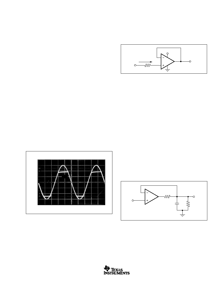
unlike some other op amps.
Normally, input bias current is approximately 1pA. How-
ever, input voltages exceeding the power supplies can
cause excessive current to flow in or out of the input pins.
Momentary voltages greater than the power supply can be
tolerated as long as the current on the input pins is limited
to 10mA. This is easily accomplished with an input resis-
tor, as shown in Figure 2.
5k
OPAx336
10mA max
+5V
V
IN
V
OUT
I
OVERLOAD
FIGURE 1. No Phase Inversion with Inputs Greater than the
Power-Supply Voltage.
FIGURE 2. Input Current Protection for Voltages Exceeding
the Supply Voltage.
FIGURE 3. Series Resistor in Unity-Gain Configuration
Improves Capacitive Load Drive.
6V
0V
V
OUT
OPA336, 2336, 4336
8
SBOS068B
www.ti.com
accuracy. For example, with R
L
= 25k
, OPA336 series op
amps perform well with capacitive loads in excess of 1000pF,
as shown in Figure 4. Without R
S
, capacitive load drive is
typically 350pF for these conditions, as shown in Figure 5.
Capacitive Load (pF)
Resistive Load (k
)
10
5
100
10k
1k
100
Operation Above Selected Gain
Curve Not Recommended
G = +1
R
L
to Ground
G = +2
R
L
to Ground
G = +1
R
L
to V
S
/2
V
S
= +5V, V
O
= V
S
/2
FIGURE 4. Small-Signal Step Response Using Series Re-
sistor to Improve Capacitive Load Drive.
Alternatively, the resistor may be connected in series with
the output outside of the feedback loop. However, if there is
a resistive load parallel to the capacitive load, it and the
series resistor create a voltage divider. This introduces a
Direct Current (DC) error at the output, however, this error
may be insignificant. For instance, with R
L
= 100k
and
R
S
= 100
, there is only about a 0.1% error at the output.
Figure 5 shows the recommended operating regions for the
OPA336. Decreasing the load resistance generally improves
capacitive load drive. Figure 5 also illustrates how stability
differs depending on where the resistive load is connected.
With G = +1 and R
L
= 10k
connected to V
S
/2, the OPA336
can typically drive 500pF. Connecting the same load to
ground improves capacitive load drive to 1000pF.
R
S
= 100
, Load = 2k
|| 1000pF, V
S
= +5V
50
µ
s/div
20mV/div
FIGURE 5. Stability--Capacitive Load vs Resistive Load.

PACKAGING INFORMATION
Orderable Device
Status
(1)
Package
Type
Package
Drawing
Pins Package
Qty
Eco Plan
(2)
Lead/Ball Finish
MSL Peak Temp
(3)
OPA2336E/250
ACTIVE
MSOP
DGK
8
250
None
CU NIPDAU
Level-1-235C-UNLIM
OPA2336E/2K5
ACTIVE
MSOP
DGK
8
2500
None
CU NIPDAU
Level-1-235C-UNLIM
OPA2336EA/250
ACTIVE
MSOP
DGK
8
250
None
CU NIPDAU
Level-1-235C-UNLIM
OPA2336EA/2K5
ACTIVE
MSOP
DGK
8
2500
None
CU NIPDAU
Level-1-235C-UNLIM
OPA2336P
ACTIVE
PDIP
P
8
50
None
Call TI
Level-NA-NA-NA
OPA2336PA
ACTIVE
PDIP
P
8
50
None
Call TI
Level-NA-NA-NA
OPA2336U
ACTIVE
SOIC
D
8
100
None
CU SNPB
Level-2-220C-1 YEAR
OPA2336U/2K5
ACTIVE
SOIC
D
8
2500
None
CU SNPB
Level-2-220C-1 YEAR
OPA2336UA
ACTIVE
SOIC
D
8
100
None
CU SNPB
Level-2-220C-1 YEAR
OPA2336UA/2K5
ACTIVE
SOIC
D
8
2500
None
CU SNPB
Level-2-220C-1 YEAR
OPA336N/250
ACTIVE
SOT-23
DBV
5
250
None
CU NIPDAU
Level-1-235C-UNLIM
OPA336N/3K
ACTIVE
SOT-23
DBV
5
3000
None
CU NIPDAU
Level-1-235C-UNLIM
OPA336NA/250
ACTIVE
SOT-23
DBV
5
250
None
CU NIPDAU
Level-1-235C-UNLIM
OPA336NA/3K
ACTIVE
SOT-23
DBV
5
3000
None
CU NIPDAU
Level-1-235C-UNLIM
OPA336NJ/250
ACTIVE
SOT-23
DBV
5
250
None
CU NIPDAU
Level-3-220C-168 HR
OPA336NJ/3K
ACTIVE
SOT-23
DBV
5
3000
None
CU NIPDAU
Level-3-220C-168 HR
OPA336P
OBSOLETE
PDIP
P
8
None
Call TI
Call TI
OPA336PA
OBSOLETE
PDIP
P
8
None
Call TI
Call TI
OPA336U
ACTIVE
SOIC
D
8
100
None
CU SNPB
Level-2-220C-1 YEAR
OPA336U/2K5
ACTIVE
SOIC
D
8
2500
None
CU SNPB
Level-2-220C-1 YEAR
OPA336UA
ACTIVE
SOIC
D
8
100
None
CU SNPB
Level-2-220C-1 YEAR
OPA336UA/2K5
ACTIVE
SOIC
D
8
2500
None
CU SNPB
Level-2-220C-1 YEAR
OPA336UJ
PREVIEW
SOIC
D
8
100
None
Call TI
Call TI
OPA336UJ/2K5
PREVIEW
SOIC
D
8
2500
None
Call TI
Call TI
OPA4336EA/250
ACTIVE
SSOP/
QSOP
DBQ
16
250
None
CU NIPDAU
Level-3-240C-168 HR
OPA4336EA/2K5
ACTIVE
SSOP/
QSOP
DBQ
16
2500
None
CU NIPDAU
Level-3-240C-168 HR
OPA4336PA
OBSOLETE
PDIP
N
14
None
Call TI
Call TI
(1)
The marketing status values are defined as follows:
ACTIVE: Product device recommended for new designs.
LIFEBUY: TI has announced that the device will be discontinued, and a lifetime-buy period is in effect.
NRND: Not recommended for new designs. Device is in production to support existing customers, but TI does not recommend using this part in
a new design.
PREVIEW: Device has been announced but is not in production. Samples may or may not be available.
OBSOLETE: TI has discontinued the production of the device.
(2)
Eco Plan - May not be currently available - please check
http://www.ti.com/productcontent
for the latest availability information and additional
product content details.
None: Not yet available Lead (Pb-Free).
Pb-Free (RoHS): TI's terms "Lead-Free" or "Pb-Free" mean semiconductor products that are compatible with the current RoHS requirements
for all 6 substances, including the requirement that lead not exceed 0.1% by weight in homogeneous materials. Where designed to be soldered
at high temperatures, TI Pb-Free products are suitable for use in specified lead-free processes.
Green (RoHS & no Sb/Br): TI defines "Green" to mean "Pb-Free" and in addition, uses package materials that do not contain halogens,
including bromine (Br) or antimony (Sb) above 0.1% of total product weight.
(3)
MSL, Peak Temp. -- The Moisture Sensitivity Level rating according to the JEDECindustry standard classifications, and peak solder
PACKAGE OPTION ADDENDUM
www.ti.com
9-Dec-2004
Addendum-Page 1

temperature.
Important Information and Disclaimer:The information provided on this page represents TI's knowledge and belief as of the date that it is
provided. TI bases its knowledge and belief on information provided by third parties, and makes no representation or warranty as to the
accuracy of such information. Efforts are underway to better integrate information from third parties. TI has taken and continues to take
reasonable steps to provide representative and accurate information but may not have conducted destructive testing or chemical analysis on
incoming materials and chemicals. TI and TI suppliers consider certain information to be proprietary, and thus CAS numbers and other limited
information may not be available for release.
In no event shall TI's liability arising out of such information exceed the total purchase price of the TI part(s) at issue in this document sold by TI
to Customer on an annual basis.
PACKAGE OPTION ADDENDUM
www.ti.com
9-Dec-2004
Addendum-Page 2

MECHANICAL DATA
MPDI001A ≠ JANUARY 1995 ≠ REVISED JUNE 1999
POST OFFICE BOX 655303
∑
DALLAS, TEXAS 75265
P (R-PDIP-T8)
PLASTIC DUAL-IN-LINE
8
4
0.015 (0,38)
Gage Plane
0.325 (8,26)
0.300 (7,62)
0.010 (0,25) NOM
MAX
0.430 (10,92)
4040082/D 05/98
0.200 (5,08) MAX
0.125 (3,18) MIN
5
0.355 (9,02)
0.020 (0,51) MIN
0.070 (1,78) MAX
0.240 (6,10)
0.260 (6,60)
0.400 (10,60)
1
0.015 (0,38)
0.021 (0,53)
Seating Plane
M
0.010 (0,25)
0.100 (2,54)
NOTES: A. All linear dimensions are in inches (millimeters).
B. This drawing is subject to change without notice.
C. Falls within JEDEC MS-001
For the latest package information, go to http://www.ti.com/sc/docs/package/pkg_info.htm


MECHANICAL DATA
MSOI004E JANUARY 1995 - REVISED MAY 2002
1
POST OFFICE BOX 655303
∑
DALLAS, TEXAS 75265
DBQ (R-PDSO-G**) PLASTIC SMALL-OUTLINE PACKAGE
4073301/F 02/2002
0.069 (1,75) MAX
Seating Plane
0.004 (0,10)
0.010 (0,25)
0.010 (0,25)
0.016 (0,40)
0.035 (0,89)
0.244 (6,20)
0.228 (5,80)
1
12
24
13
0.150 (3,81)
0.157 (3,99)
0.008 (0,20) NOM
0
∞
-8
∞
Gauge Plane
0.012 (0,30)
0.008 (0,20)
0.197
(5,00)
(4,80)
0.189
A MAX
A MIN
PINS **
DIM
16
0.337
(8,56)
(8,74)
0.344
20
24
A
(8,74)
0.344
(8,56)
0.337
28
0.394
(10,01)
0.386
(9,80)
M0-137
VARIATION
AB
AD
AE
AF
D
0.025 (0,64)
0.005 (0,13)
0.004 (0,10)
NOTES: A. All linear dimensions are in inches (millimeters).
B. This drawing is subject to change without notice.
C. Body dimensions do not include mold flash or protrusion not to exceed 0.006 (0,15).
D. Falls within JEDEC MO-137.

IMPORTANT NOTICE
Texas Instruments Incorporated and its subsidiaries (TI) reserve the right to make corrections, modifications,
enhancements, improvements, and other changes to its products and services at any time and to discontinue
any product or service without notice. Customers should obtain the latest relevant information before placing
orders and should verify that such information is current and complete. All products are sold subject to TI's terms
and conditions of sale supplied at the time of order acknowledgment.
TI warrants performance of its hardware products to the specifications applicable at the time of sale in
accordance with TI's standard warranty. Testing and other quality control techniques are used to the extent TI
deems necessary to support this warranty. Except where mandated by government requirements, testing of all
parameters of each product is not necessarily performed.
TI assumes no liability for applications assistance or customer product design. Customers are responsible for
their products and applications using TI components. To minimize the risks associated with customer products
and applications, customers should provide adequate design and operating safeguards.
TI does not warrant or represent that any license, either express or implied, is granted under any TI patent right,
copyright, mask work right, or other TI intellectual property right relating to any combination, machine, or process
in which TI products or services are used. Information published by TI regarding third-party products or services
does not constitute a license from TI to use such products or services or a warranty or endorsement thereof.
Use of such information may require a license from a third party under the patents or other intellectual property
of the third party, or a license from TI under the patents or other intellectual property of TI.
Reproduction of information in TI data books or data sheets is permissible only if reproduction is without
alteration and is accompanied by all associated warranties, conditions, limitations, and notices. Reproduction
of this information with alteration is an unfair and deceptive business practice. TI is not responsible or liable for
such altered documentation.
Resale of TI products or services with statements different from or beyond the parameters stated by TI for that
product or service voids all express and any implied warranties for the associated TI product or service and
is an unfair and deceptive business practice. TI is not responsible or liable for any such statements.
Following are URLs where you can obtain information on other Texas Instruments products and application
solutions:
Products
Applications
Amplifiers
amplifier.ti.com
Audio
www.ti.com/audio
Data Converters
dataconverter.ti.com
Automotive
www.ti.com/automotive
DSP
dsp.ti.com
Broadband
www.ti.com/broadband
Interface
interface.ti.com
Digital Control
www.ti.com/digitalcontrol
Logic
logic.ti.com
Military
www.ti.com/military
Power Mgmt
power.ti.com
Optical Networking
www.ti.com/opticalnetwork
Microcontrollers
microcontroller.ti.com
Security
www.ti.com/security
Telephony
www.ti.com/telephony
Video & Imaging
www.ti.com/video
Wireless
www.ti.com/wireless
Mailing Address:
Texas Instruments
Post Office Box 655303 Dallas, Texas 75265
Copyright
2004, Texas Instruments Incorporated